Lab
for Silicon Solar Cells Research at the Atominstitut
* Processing
from silicon wafer to finished solar cell
* Emitter formation in diffusion furnaces using POCL3
* Back side Al/Ag screen printing
* Front side contacting: * screen printing
* or fully autiomated grain boundary detection and outlining with dispenser
* or evaporation and galvanic thickening
|
|
|
|
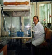
Loading wafers into quartz boat for POCl-diffusion
|
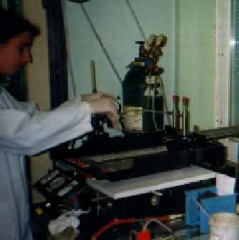
Screen printing of Al/Ag-paste on back side
|
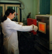
Firing of Al/Ag-paste on back side
|
Back
* Characterisation:
* Measurement of minority carrier lifetime by photo-conductance decay
* Automatic detection of grain boundaries by optical means and by LBIC
* Profiling of sheet resistance of emitter
* Profiling of voltage across surface area of illuminated solar cell
* Light-beam induced current measurement with high position resolution
for cells with and without front metal contacts
* Contact resistance measurements of metal fingers
* Current-voltage characteristics of finished cell
* Automated daylight logging and artificial illumination of up to 100 Watts
modules and detailed IV-analysis
|
|
|
|
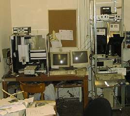
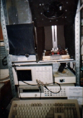
Characterisation corner
|
Lifetime (left) and current-voltage (right) measurement
|
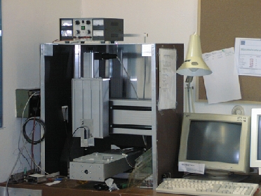
XYZ-workhorse: Sheet resistance profiling, LBIC profiling, Contact
resistance measurements, Surface voltage profiling
|
|
|
|
|
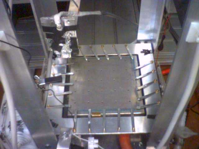
LBIC system for cells without front metallisation
|
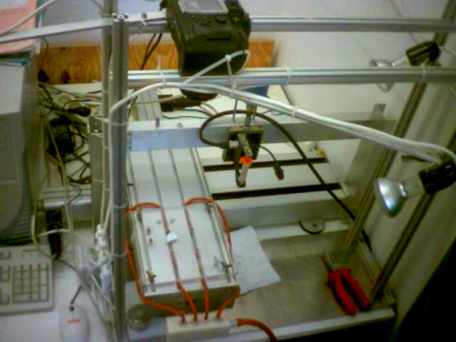
Plotting system for detecting grain boundaries and writing metal
lines along selected grain boundaries
|
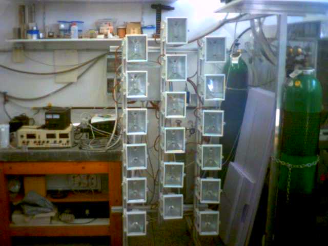
9 kW Illumination array for testing modules
|
Back
Changes 30.March.2004 by J.Summhammer