OPTIMISATION OF ARTISTIC CONTACT PATTERNS ON MULTICRYSTALLINE SILICON SOLAR
CELLS
M. Radike, J.
Summhammer
Atominstitut der Österreichischen Universitäten, Stadionallee
2, A-1020 Wien, Austria
Tel: +43-1-58801-14112, Fax: +43-1-58801-14199, Email: mradike@ati.ac.at
or summhammer@ati.ac.at
A. Breymesser, V.
Schlosser
Institut für Materialphysik, Universität Wien, Boltzmanngasse
9, 1090 Wien, Austria
ABSTRACT:
The acceptance of photovoltaic modules in highly visible places like walls
and roofs of buildings, or for small scale village use, is in a large part
determined by nontechnical aspects, most of all by the visual appeal. The
design of the surfaces of cells and modules must therefore meet two optimization
criteria: High energetic output and attractive appearance. As the bus bars
of the front collection grid are often considered visually annoying, we
have tried to convert them into an asset by incorporating artistic shapes
into them. Ten different designs have been analysed and screen printed
onto 103 x 103 mm2 multicrystalline Si solar cells. For a 15
% efficient cell with standard H-pattern we have found that it would at
worst be reduced to an efficiency of 14.5 % when equipped with one of our
artistic bus bar designs.
Keywords: Multi-Crystalline - 1: Busbars - 2: Building Integration -
3
1 INTRODUCTION
Photovoltaic research is usually centred around conversion efficiency.
However, for a wide dissemination, it seems necessary not only to have
high efficiency, but to offer panels which are aesthetically pleasing and
attractive to look at. This may be particularly true for building integration,
small scale village use, or private use.
The goal of attractive appearance can be achieved in many ways. In
the present work we have focussed on the design of the bus bars on the
front side of 100 x 100 mm2 crystalline silicon cells, but the
results are valid more generally. We have chosen the bus bars, because
they are lines of sufficient thickness to be noticeable even from the distance.
Currently they are mainly straight, which is, more often than not, perceived
as disturbing. More interesting patterns might convert bus bars from a
nuisance to an asset, which could be further enhanced by colouring them
with an appropriate solder alloy.
We have created nine new patterns and modified the fine finger grid
where necessary. It turns out that the loss in efficiency due to additional
shading can be expected to be at most 0.5% absolute, and the loss due to
additional serial resistance will be below 0.1% absolute, both for 15%
efficiency with the standard bus bar pattern. All of the patterns have
also been screen printed on real multicrystalline cells and subjected to
first experimental tests.
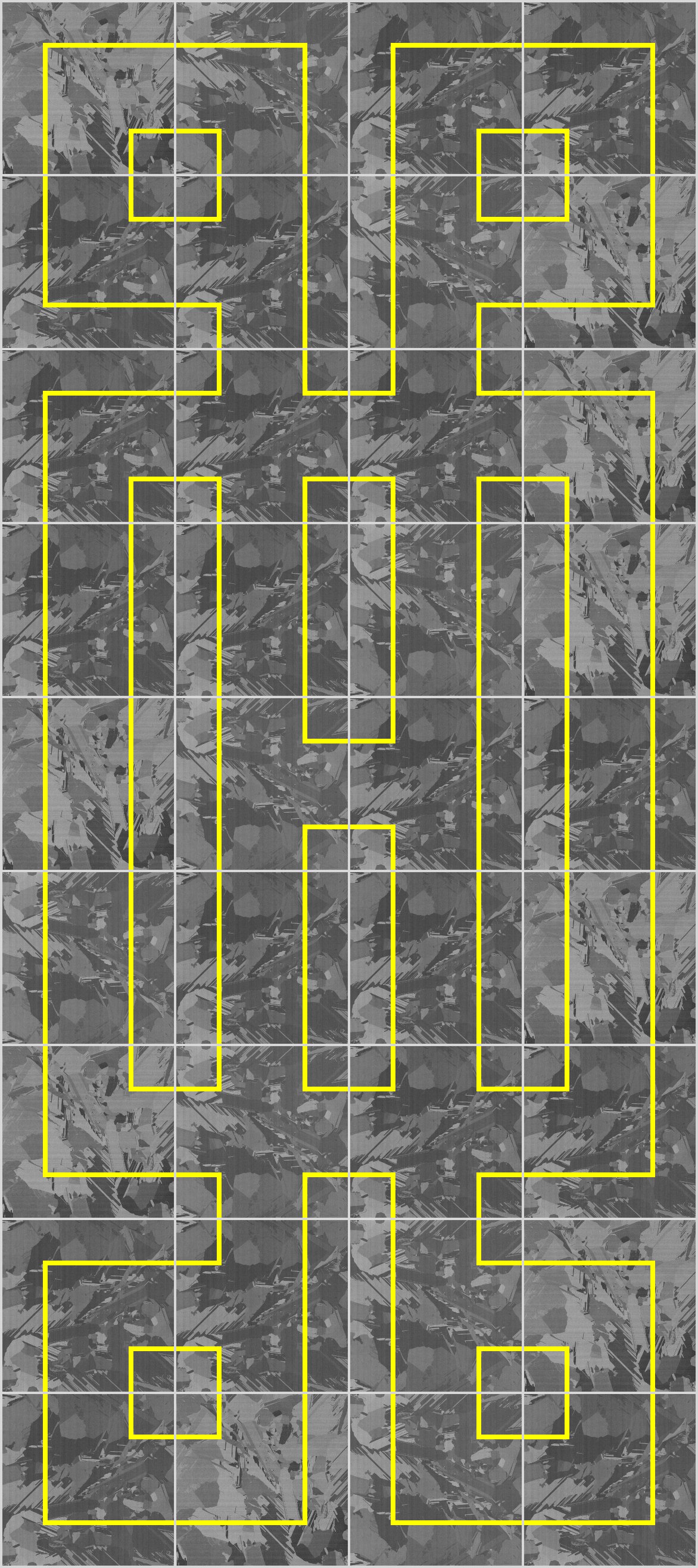
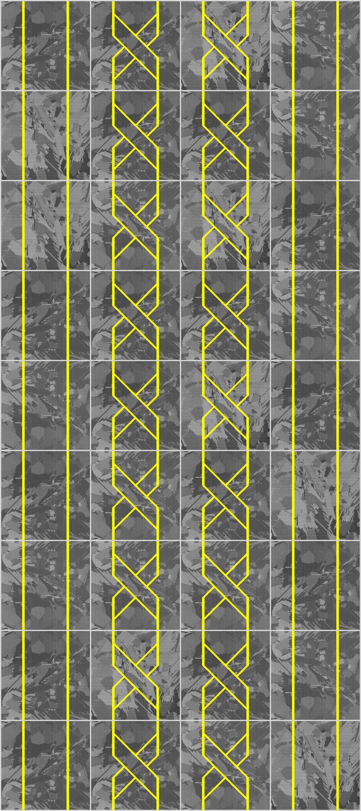
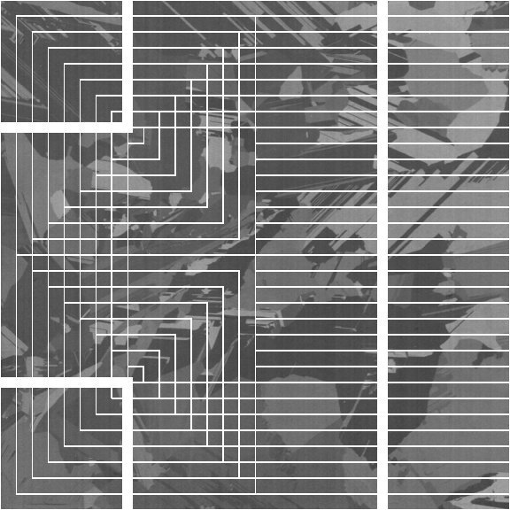
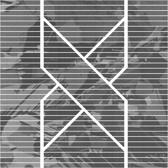
2 DESIGNS
The designs are shown in Fig.1. The basic concept was to "see the module,
not just the cell". The bus bars were thus designed with the intention
to permit a wide variety of overall bus bar patterns of the module with
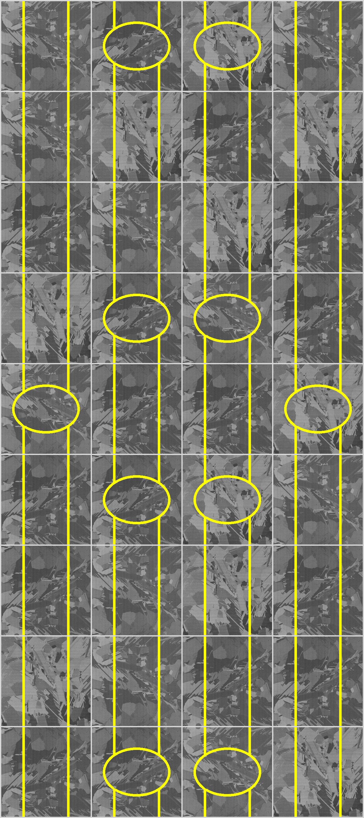
just a few elementary cell patterns. For instance, patterns 1 - 4 allow
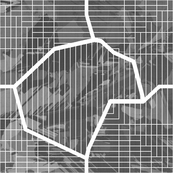
to create any combination of quadratic and rectangular patterns. (Panel
1 in Fig.2.) Including the patterns 5 - 8 increases the range of possibilities.
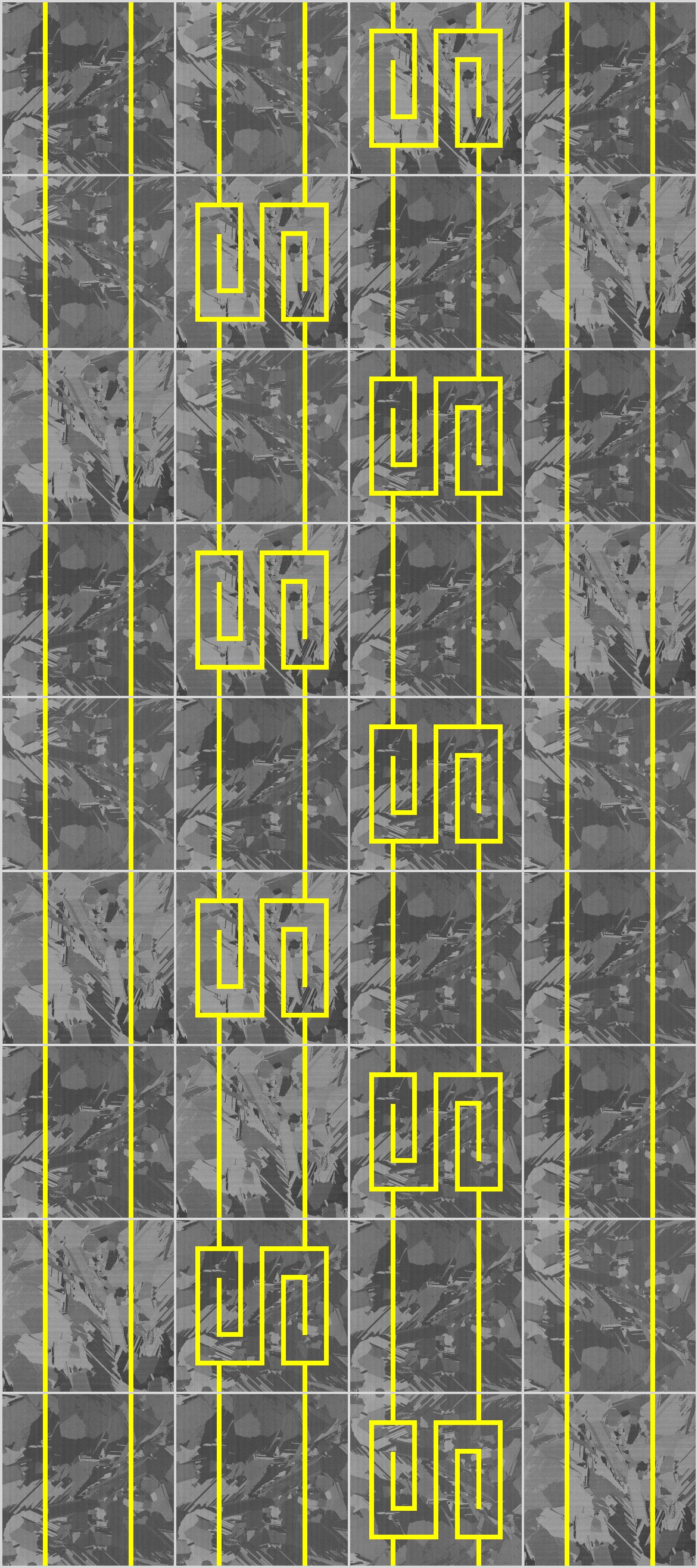
(Panels 2 and 3 in Fig.2.) An attempt to break out of the "two bus bars"-principle
was made with patterns 9 and 10. Pattern 9 (Crack) has connection points
in the middle of the four sides of the wafer, but the inner layout of the
bus bar is fully asymmetric. This permits a tremendous number of ordered
as well as chaotic patterns in a panel with just a single cell type! (Panel
4 in Fig.2). Clearly, electrical series connection between cells in a module
cannot always be as the bus bar pattern suggests. Sometimes leads will
have to be isolated and run underneath a few cells to the next connection.
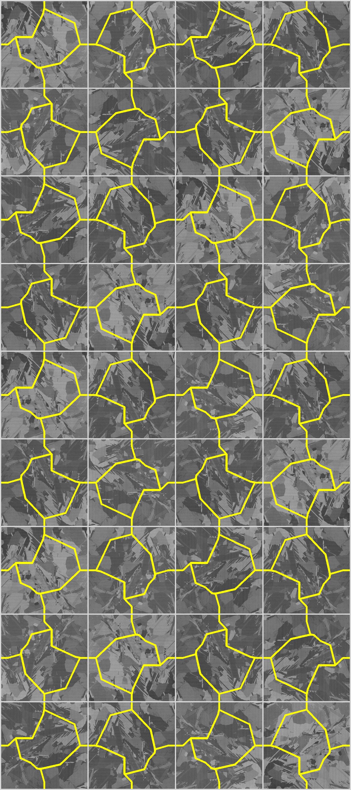
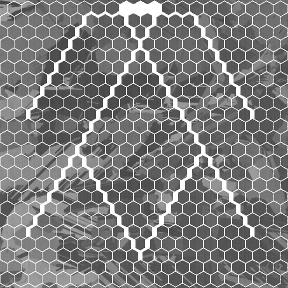
Pattern 10 (Hexagon) is an attempt to obtain less visible bus bars, by
having a hexagonal finger web and thinner bus lines.
All designs were made with a resolution of 600 dots per inch. Finger
thickness was 2 dots (85 µm). Bus bar thickness in patterns 1 - 9
was 48 dots (2.03 mm), and center-center distance of fingers was 72 dots
(3.05 mm). In pattern 10 the side of a hexagon is 65 dots (2,75 mm), and
the bus bar thickness is 35 dots (1,48 mm). The theoretical efficiencies
as modified by additional shading, on the basis of 15% efficiency with
the standard pattern, are shown in Table I.The theoretical shading caused
by the patterns is shown in Table II.
Figure 1: Front contact patterns
|

|
|
|
|
| 1: Standard |
2: L |
3: Cross |
4: T |
5: Sinus |
 |
 |
 |
 |
 |
| 6: Delhi |
7: Ellipse |
8: Braid |
9: Crack |
10: Hexagon |
3 THEORY
Aside from losses due to additional shading, any deviation from the standard
pattern 1 can be expected to give rise to additional resistive losses,
which may be partly offset by reduced contact resistance losses. In patterns
(5), (6), (7) and (8) we can expect negligible additional series resistance
losses compared to standard pattern 1. For instance, take pattern 5 (Sinus).
It is designed to give exactly the same shading as the standard pattern,
by making the bus bars marginally thinner. We will neglect resistive losses
in the bus bars. The resistive losses in the fingers between the bus bars
will be the same as in the standard pattern. Those in the fingers on the
right will be larger, and those in the fingers on the left will be smaller,
than in the standard pattern. The power loss in such a finger is given
by [1] as
Ploss = Rholf (j2 d2
b3)/3
where Rholf is the resistance per unit length of the finger,
j is the generated current per unit area, d is the distance between the
fingers, and b is the length of the finger to the bus bar. For Rholf
= 0.6 Ohm/cm and j = 340 A/m2 we find for our parameters a total
loss in the external fingers of pattern 5 of 22 mW, while the corresponding
loss in standard pattern 1 is 18 mW.
A cell of 15 % efficiency with the standard pattern would thus show
an efficiency of 14.95 % with pattern Sinus.
More losses can be expected in pattern 3 (Cross), if the contact is
made in the traditional way to the bus bar exits on one side. Then a major
portion of the power must be transported through the fingers. An upper
limit estimate is the assumption that all power is collected and transported
through 16 fingers over a distance of 100 mm. There would be a loss of
90 mW, or about 6 % of the generated power. However, with interconnections
of the bus bars of the cell by wires underneath the cell the resistive
losses will be comparable to or less than those in the standard pattern.
Similar conclusions apply to pattern 4 (T).
Table I: Theoretical efficiency using different new grid patterns
in comparison to the standard grid (1).
| Pattern |
Theoretical efficiency (%) |
| 1 Standard |
15.00 (defined) |
| 2 L |
14.95 |
| 3 Cross |
14.92 |
| 4 T |
14.96 |
| 5 Sinus |
14.95 |
| 6 Delhi |
14.70 |
| 7 Ellpise |
14.72 |
| 8 Braid |
14.63 |
| 9 Crack |
14.65 |
| 10 Hexagon |
14.52 |
The additional series resistances in pattern 2 (L) and in pattern 9
(Crack) will lead to a decrease in efficiency below 0.1 % absolute relative
to a 15 % efficient cell with standard pattern. Pattern 10 (Hexagon) could
not yet by treated analytically. The sheet resistance of the emitter will
play a role, because the innermost points of each finger hexagon have a
farther path to the finger web than in any other pattern. On the other
hand, a larger fraction of points than in the other patterns is within
intermediate distances to the web. Moreover, current flow will be more
homogeneous in the fingers, thereby avoiding peaked I2R-losses.
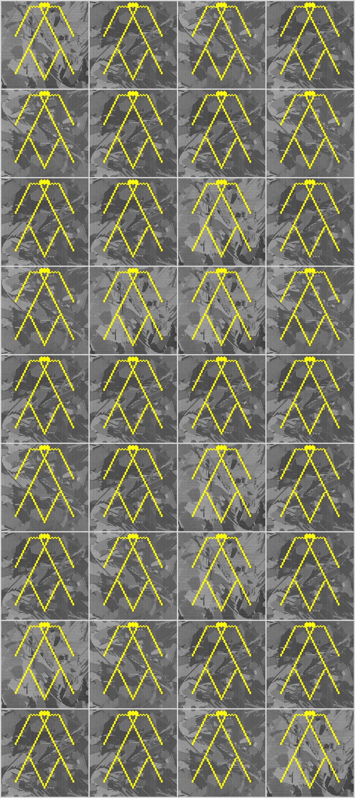
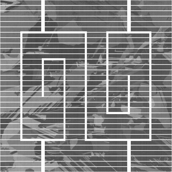
Figure 2: The possible look of future modules
4 Experiments
Multicrystalline Eurosolare 103 x 103 mm2 silicon wafers of
340 µm thickness and 1.5 Ohm.cm specific resistivity were POCl3-diffused
at 840 °C (30 min vapour, 60 min drive in). Exploiting the characteristics
of the oven, four groups of sheet resistances were produced: 60-70, 70-80,
80-95 and 95 to 130 Ohm/square. The rear side was aluminised by screen
printing and diffused to obtain good contact and back surface field. The
front grid patterns were screen printed with commercial silver paste using
screens of 200 threads/cm. The horizontal lines of the patterns were rotated
by 22 degrees relative to the threads. Since screen printing is sensitive
to mechanical parameters, we tried to keep the speed of the squeegee, which
was pulled by hand, to 1cm/s.
The actual shading after screen printing was determined by scanning
each cell with a commercial scanner with a resolution of 600 dots per inch
to obtain an image in 256 steps of grey. The screen printed lines appear
relatively white, such that the pixels representing lines could be counted
automatically, thereby accepting an error of mistaking bright areas of
some grains as silver lines. The most probable values are shown in Column
"Printed shading" in Table II. They have an uncertainty towards larger
values, but certainly do not exceed the upper limits given in column 4
of Table II. The numbers suggest still non-optimal viscosity of the paste
and perhaps screen thread density [2,3].
Four-point resistance measurements under reverse bias as well as non-bias
conditions have also been made on many fingers on the cells. Patterns 1-9
still had many interruptions. However, pattern 10, whose finger grid is
a hexagonal web, showed almost no interruptions. On this pattern, resistance
from anywhere on the fingers to the nearest bus bar point always was below
250mOhm. This is explained by the many paths leading from one point to
any other in this web.
Table II: Theoretical and practical values of the area shaded
by pattern grid lines in percent compared to 100 x 100 mm²:
| Pattern |
Theoretical shading (%) |
Printed shading (%) |
Upper limit (%) |
| Standard |
6.50 |
9.2 |
10.2 |
| L |
6.79 |
9.4 |
10.5 |
| Cross |
6.99 |
10.0 |
11.3 |
| T |
6.78 |
9.5 |
10.6 |
| Sinus |
6.50 |
9.4 |
10.4 |
| Delhi |
8.40 |
10.7 |
11.7 |
| Ellipse |
8.22 |
10.6 |
11.7 |
| Braid |
8.83 |
11.2 |
12.2 |
| Crack |
8.67 |
11.0 |
12.0 |
| Hexagon |
9.51 |
11.8 |
12.8 |
5 Conclusion
We have introduced new bus bar patterns with the explicit goal of enhancing
the visual appeal of crystalline silicon solar cells and modules. We showed
that the fear of a large loss in efficiency is unfounded. The expected
loss in efficiency is mainly due to additional shading and is less than
0.5% absolute for cells which would show 15% efficiency with the standard
bus bar pattern. Resistive losses in the changed finger grid would amount
to an efficiency loss well below 0.1% absolute.
ACKNOWLEDGMENT
Part of this work is supported by Joule Project Nr. JOR3CT970175 under
the coordination of BP Solar Ltd.
REFERENCES
[1] A.R. Burgers, J.A. Eikelboom, "Optimizing metalization patterns for
yearly yield", Proceedings of the 26-th IEEE Photovoltaic Specialists Conference,
219.
[2] J. Hoornstra, A.W. Weeber, H.H.C. de Moor, W.C. Sinke, "The importance
of paste rheology in improving fine line, thick film screen printing of
front side metallization", Proceedings of the 14th European Photovoltaic
Solar Energy Conference, 823.
[3] D. Dziedzic, J. Nijs and J. Szlufcik, Hybrid Circuits, No.30, January
1993.
Changes 2.Apr.2001 by J.Summhammer