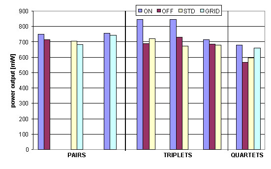
"ON-cell" and "OFF-cell"
"STD-cell" and "GRID-cell"
In the present work another method has been investigated. The metallic front contact pattern of mc Silicon solar cells were put over and along grain boundaries (grain boundary oriented finger grid, GBOF). The front contact patterns were applied galvanically using nickel as a diffusion barrier and silver as the conductor, in view of a possible application in laser grooved buried contact cells.
The study was done on Baysix 100 x 100 mm2 wafers of about 270 µm thickness, which were boron doped between 0.5 and 2.0 Ohm.cm. Several batches of up to 80 wafers each were processed. Four different kinds of front contact patterns were investigated: ON, OFF, STD and GRID. There were four different studies: - Triplets study: ON - OFF - STD; - Quartets study: ON - OFF- STD - GRID; - Pairs study: ON - OFF; STD - GRID and ON - GRID.
The typical fraction of grid length on grain boundaries was about 77 % for ON-cells whereas it was only between 25 % and 30 % for OFF- and GRID-cells. For the STD-cells it was about 25 %. The detection of the grain boundaries was done by optical contour tracing methods.
The cells received no passivation of surfaces and grain boundaries and no antireflection coating.
Under AM1.5 conditions the ON-cells showed an efficiency increase of over 5 % relative to the OFF- and STD-cells and an increase of about 3 % relative to the GRID-cells. They also had a higher fill factor, sometimes exceeding 80 %, a higher short circuit current and a lower series resistance.
The next figure shows quite clearly that the ON-cells outperform the other types in terms of power output.